Kilas Balik
• Arsitektur von Neumann
– Jadi acuan baku sistem komputer modern.
– Instruksi & data dicampur dalam memori yang sama,
dengan keuntungan:
• Efficient use of memory --- you have 1 large block that can
be used any way you want instead of 2 smaller blocks.
• Computers can handle instructions as easily as data ---
since instructions and data are stored together, moving blocks
of instructions (i.e. programs) around becomes simple.
• Ease of loading programs into memory --- just read the
instructions in as data from disk or other long-term storage and
then execute the newly-read information.
IF-ITB/Santika WP/Maret08
IF2291 – Tekonologi Prosesor
Page 3
Kilas Balik
• Arsitektur von Neumann
– Selain menguntungkan juga merugikan, karena:
• Data can overwrite instructions --- without special
hardware precautions (called memory protection), an incorrect
write to memory could overwrite some instructions. Since Von
Neumann systems don't distinguish between instructions and
data, the computer would attempt to execute the data as
instructions, usually with an undesired result.
• Limited bandwidth --- storing instructions and data together
means they both follow the same path to get to the processor.
This Von Neumann Bottleneck means that the processor has to
trade off between executing a large number of instructions per
second and reading in a large amount of data in the same
time.
IF-ITB/Santika WP/Maret08
IF2291 – Tekonologi Prosesor
Page 4
Kilas Balik
• Kinerja vs Desain Prosesor
– Performance komputer ditentukan oleh
• Instruction count.
• Clock cycle time.
• Clock cycles per instruction.
– Processor design (datapath & control)
akan ditentukan oleh
• Clock cycle time.
• Clock cycles per instruction.
IF-ITB/Santika WP/Maret08
IF2291 – Tekonologi Prosesor
Page 5
Proses Instruksi
• Siklus Dasar
– Execute Cycle, kategori
• CPU – Memory : Data ditransfer dari M ke CPU atau
sebaliknya. {IR [adres] <=> MAR }
• CPU - I/O : Data ditransfer dari modul I/O atau
sebaliknya. {MAR => Memory => MBR }
• Data Processing : CPU mengerjakan operasi
aritmatika / logika pada data via ALU. {MBR =>
ACC }
• Control.
IF-ITB/Santika WP/Maret08
IF2291 – Tekonologi Prosesor
Page 6
Proses Instruksi
• Siklus Dasar
– Ilustrasi operasi ADD
• IR [adres] => MAR
• MAR => Memory => MBR
• MBR + ACC => ALU
• ALU => ACC
– Interrupt Cycle ~ mekanisme di mana suatu
modul I/O dsb., dapat menghentikan kendali
runtutan operasi normal CPU.
– Interupsi dilakukan oleh program, timer, I/O, &
hardware failure.
IF-ITB/Santika WP/Maret08
IF2291 – Tekonologi Prosesor
Page 7
Desain Prosesor
• Analisa instruction set untuk menghasilkan datapath
sesuai kebutuhan.
– Arti setiap instruksi diuraikan dari register transfers.
– Datapath harus mencakup elemen storage untuk registerregister
ISA.
– Datapath juga harus menunjang setiap register transfer.
• Pilih sekumpulan datapath components & tetapkan
metodologi clocking.
• Implementasi datapath yang dibutuhkan.
• Analisa implementasi setiap instruksi untuk
menentukan setting of control points yang akan
mempengaruhi register transfer.
• Implementasi control logic.
IF-ITB/Santika WP/Maret08
IF2291 – Tekonologi Prosesor
Page 8
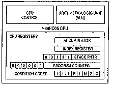
Desain Prosesor
Eksekusi instruksi lw $1,0($2) :
– CU sets the multiplexor to drive the PC onto the address bus.
– M responds by placing 8c410000 (hexa) on the data bus from
where it is latched into the IR.
– CU decodes the instruction, at the same time it instructs the
ALU.
– Output from the ALU is latched into the MAR.
– M responds with the value sought, it is captured on the
internal data bus and latched into register 1 of the register
file.
– PC is now updated to point to the next instruction and the
cycle can start again.
IF-ITB/Santika WP/Maret08
IF2291 – Tekonologi Prosesor
Page 9
Desain Prosesor
• Format instruksi MIPS [PAT97]
– Tipe-R
– Tipe-I
– Tipe-J
• Keterangan
– Shamt: shift amount.
– Funct: pilih jenis operasi pada “op” field.
– Immediate: address offset atau immediate value.
– Target address: adres tujuan karena jump instruction.
op rs rt rd shamt funct
31 26 21 16 11 6 0
6 bits 5 bits 5 bits 5 bits 5 bits 6 bits
op rs rt immediate
31 26 21 16 0
6 bits 5 bits 5 bits 16 bits
op target address
31 26 0
6 bits 26 bits
IF-ITB/Santika WP/Maret08
IF2291 – Tekonologi Prosesor
Page 10
Teknologi
• Tujuan Desainer Komputer
– Menciptakan sistem yang
• As fast as possible.
• As inexpensive as possible.
• as powerful as possible.
– Kinerja sistem tergantung pada
• Memory
• Processor
• Connection to the peripheral devices.
• Actual peripherals.
IF-ITB/Santika WP/Maret08
IF2291 – Tekonologi Prosesor
Page 11
Teknologi
• CISC http://physinfo.ulb.ac.be/divers_html
– Philosophy for designing chips that are easy to
program and which make efficient use of
memory.
– Each instruction in a CISC instruction set might
perform a series of operations inside the
processor. This reduces the number of
instructions required to implement a given
program, and allows the programmer to learn a
small but flexible set of instructions.
IF-ITB/Santika WP/Maret08
IF2291 – Tekonologi Prosesor
Page 12
Teknologi
• CISC, Filosofi-1: Microcode
– Microprogrammed system, main processor has some builtin
memory (typically ROM) which contains groups of
microcode instructions which correspond with each
machine-language instruction.
– Keuntungan Sistem Microprogrammed
• Since the microcode memory can be much faster than main
memory, an instruction set can be implemented in microcode
without losing much speed over a purely hard-wired
implementation.
• New chips are easier to implement and require fewer transistors
than implementing the same instruction set with dedicated logic.
• A microprogrammed design can be modified to handle entirely
new instruction sets quickly.
IF-ITB/Santika WP/Maret08
IF2291 – Tekonologi Prosesor
Page 13
Teknologi
• CISC, Filisofi-2: Build "rich" instruction
sets.
– Designers could build more functionality into each
instruction.
– Cut down on the total number of instructions
required to implement a program, and therefore
made more efficient use of a slow main memory.
– Assembly-language programs life simpler.
– Designers were enhancing their instruction sets
such as: string manipulation operations, special
looping constructs, and special addressing modes
for indexing through tables in memory.
IF-ITB/Santika WP/Maret08
IF2291 – Tekonologi Prosesor
Page 14
Teknologi
• CISC, Filosofi-3: Build high-level
instruction sets.
– Once designers started building programmerfriendly
instruction sets, the logical next step was
to build instruction sets which map directly from
high-level languages.
– Not only does this simplify the compiler writer's
task, but it also allows compilers to emit fewer
instructions per line of source code.
IF-ITB/Santika WP/Maret08
IF2291 – Tekonologi Prosesor
Page 15
Teknologi
• Karakteristik instruction sets CISC
– A 2-operand format, where instructions have a source and a
destination. For example, the add instruction "add #5, D0" would add
the number 5 to the contents of register D0 and place the result in
register D0.
– Register to register, register to memory, and memory to register
commands.
– Multiple addressing modes for memory, including specialized modes
for indexing through arrays.
– Variable length instructions where the length often varies according to
the addressing mode.
– Instructions which require multiple clock cycles to execute. If an
instruction requires additional information before it can run (for
example, if the processor needs to read in two memory locations
before operating on them), collecting the extra information will
require extra clock cycles. As a result, some CISC instructions will
take longer than others to execute.
IF-ITB/Santika WP/Maret08
IF2291 – Tekonologi Prosesor
Page 16
Teknologi
• Arsitektur CISC
– Complex instruction-decoding logic, driven by the need for a single
instruction to support multiple addressing modes.
– A small number of general purpose registers. This is the direct result
of having instructions which can operate directly on memory and the
limited amount of chip space not dedicated to instruction decoding,
execution, and microcode storage.
– Several special purpose registers. Many CISC designs set aside special
registers for the stack pointer, interrupt handling, and so on. This can
simplify the hardware design somewhat, at the expense of making
the instruction set more complex.
– A Condition code register which is set as a side-effect of most
instructions. This register reflects whether the result of the last
operation is less than, equal to, or greater than zero, and records if
certain error conditions occur.
IF-ITB/Santika WP/Maret08
IF2291 – Tekonologi Prosesor
Page 17
Teknologi
• Kelemahan CISC
– Earlier generations of a processor family generally were contained as
a subset in every new version --- so instruction set & chip hardware
become more complex with each generation of computers.
– So that as many instructions as possible could be stored in memory
with the least possible wasted space, individual instructions could be
of almost any length---this means that different instructions will take
different amounts of clock time to execute, slowing down the overall
performance of the machine.
– Many specialized instructions aren't used frequently enough to justify
their existence --- approximately 20% of the available instructions are
used in a typical program.
– CISC instructions typically set the condition codes as a side effect of
the instruction. Not only does setting the condition codes take time,
but programmers have to remember to examine the condition code
bits before a subsequent instruction changes them.
IF-ITB/Santika WP/Maret08
IF2291 – Tekonologi Prosesor
Page 18
Teknologi
• RISC (Reduce Instruction Set Computer),
muncul karena:
– Semiconductor technology began to reduce the
difference in speed between main memory and
processor chips.
– As memory speed increased, and high-level
languages displaced assembly language, the
major reasons for CISC began to disappear,
and computer designers began to look at ways
computer performance could be optimized
beyond just making faster hardware.
IF-ITB/Santika WP/Maret08
IF2291 – Tekonologi Prosesor
Page 19
Teknologi
• Karakteristik RISC
– Simple instruction set.
• In a RISC machine, the instruction set contains simple,
basic instructions, from which more complex
instructions can be composed.
– Same length instructions.
• Each instruction is the same length, so that it may be
fetched in a single operation.
– 1 machine-cycle instructions.
• Most instructions complete in one machine cycle,
which allows the processor to handle several
instructions at the same time. This pipelining is a key
technique used to speed up RISC machines.
IF-ITB/Santika WP/Maret08
IF2291 – Tekonologi Prosesor
Page 20
Teknologi
• Desain RISC
– Teknik Kunci: Pipelining is a design technique
where the computer's hardware processes more
than one instruction at a time, and doesn't wait
for one instruction to complete before starting
the next.
– Four stages in CISC machine (fetch, decode,
execute, and write) are also exist in a RISC
machine, but the stages are executed in parallel.
As soon as one stage completes, it passes on the
result to the next stage and then begins working
on another instruction.
IF-ITB/Santika WP/Maret08
IF2291 – Tekonologi Prosesor
Page 21
Teknologi
• Performance issues in pipelined systems
– Memory speed issues are commonly solved using caches.
– Instruction Latency:
• Highly encoded instructions---such as those used on CISC machines--
-that require a ulating and testing thed of cal to decode
• Variable-length instructions which require multiple references to
memory to fetch in the entire instruction.
• Instructions which access main memory (instead of registers), since
main memory can be slow
• Complex instructions which require multiple clocks for execution
(many floating-point operations, for example.)
• Instructions which need to read and write the same register. For
example "ADD 5 to register 3" had to read register 3, add 5 to that value,
then write 5 back to the same register (which may still be "busy" from
the earlier read operation, causing the processor to stall until the register
becomes available.)
• Dependence on single-point resources such as a condition code
register. If one instruction sets the conditions in the condition code
register and the following instruction tries to read those bits, the second
instruction may have to stall until the first instruction's write completes.
IF-ITB/Santika WP/Maret08
IF2291 – Tekonologi Prosesor
Page 22
Teknologi
• Performance issues in pipelined systems
– Since each instruction takes some amount of
time to store its result, and several instructions
are being handled at the same time, later
instructions may have to wait for the results of
earlier instructions to be stored.
– However, a simple rearrangement of the
instructions in a program (called
Instruction Scheduling) can remove these
performance limitations from RISC programs.
IF-ITB/Santika WP/Maret08
IF2291 – Tekonologi Prosesor
Page 23
Teknologi
• Keuntungan RISC
– Speed. Since a simplified instruction set allows for a pipelined,
superscalar design RISC processors often achieve 2 to 4 times the
performance of CISC processors using comparable semiconductor
technology and the same clock rates.
– Simpler hardware. Because the instruction set of a RISC
processor is so simple, it uses up much less chip space; extra
functions, such as memory management units or floating point
arithmetic units, can also be placed on the same chip. Smaller
chips allow a semconductor manufacturer to place more parts on
a single silicon wafer, which can lower the per-chip cost
dramatically.
– Shorter design cycle. Since RISC processors are simpler than
corresponding CISC processors, they can be designed more
quickly, and can take advantage of other technological
developments sooner than corresponding CISC designs, leading to
greater leaps in performance between generations.
IF-ITB/Santika WP/Maret08
IF2291 – Tekonologi Prosesor
Page 24
Pipeline
• Teknik implementasi pada CPU untuk menaikkan
kinerja.
• Mirip proses perakitan di pabrik.
• Idea dasar pipeline adalah:
– Sementarainstruksi pertama dieksekusi.
– Instruksi kedua dapat di-fetch.
– Dikenal dengan instruction overlap.
• Model
– Simple three-stage pipeline.
– Extended pipeline.
– Superscalar.
IF-ITB/Santika WP/Maret08
IF2291 – Tekonologi Prosesor
Page 25
Pipeline
Dekomposisi Pengolahan Instruksi
– Instruction Fetch
Fetch the instruction from memory.
– Decode and Operand Fetch, decode instruction and
fetch operands from the register file.
– Execute the instruction in the ALU.
– WriteBack, write the result back in to a register.
IF-ITB/Santika WP/Maret08
IF2291 – Tekonologi Prosesor
Page 26
Pipeline
• Hambatan Desain
– Overhead tiap tahap pipeline, pada pemindahan data antar
buffer dan saat persiapan & pengiriman fungsi-fungsi operasi.
– Akibat banyak tahapan maka jumlah kendali logika naik, untuk
menangani ketergantungan memori & register serta
optimalisasi.
• Penanganan branching
– Multiple Streams
– Prefetch Branch Target
– Loop Buffer
– Branch Prediction
– Delayed Branch
IF-ITB/Santika WP/Maret08
IF2291 – Tekonologi Prosesor
Page 27
Pipeline
• Apa superscalar ?
– Instruksi-instruksi umum (arithmetic, load/store,
conditional branch) may be initiated & executed
independently.
– Dapat diterapkan pada RISC & CISC secara praktis
biasanya RISC.
• Mengapa superscalar ?
– Kebanyakan operasi pada satuan scalar.
– Dapat dibuktikan dengan implementasi
superscalar.
IF-ITB/Santika WP/Maret08
IF2291 – Tekonologi Prosesor
Page 28
Pipeline
• Apa Superpipelined ?
– Banyak tahapan pipeline memerlukan kurang dari
setengah clock cycle.
– Kecepatan ganda internal clock menghasilkan 2 tasks per
external clock cycle.
– Superscalar yang memungkinkan parallel fetch execute.
• Limitasi superscalar
– Instruction level parallelism & compiler based optimisation.
– Teknis Hardware.
– Dibatasi oleh: True data dependency, Procedural
dependency, Resource conflicts, Output dependency,
Antidependency.
IF-ITB/Santika WP/Maret08
IF2291 – Tekonologi Prosesor
Page 29
Pipeline
• True data dependency
– ADD r1, r2 (r1 := r1+r2;)
– MOVE r3,r1 (r3 := r1;)
– Dapat fetch & decode instruksi pertama & kedua secara
paralel.
– Tidak dapat mengeksekusi instruksi kedua sebelum yang
pertama selesai.
• Procedural dependency
– Tidak dapat mengeksekusi instructions after a branch in parallel
with instructions before a branch.
– Juga, jika panjang instruksi tidak pasti maka harus di-decode
dulu agar tahu berapa jumlah fetch diperlukan.
– Hal ini untuk melindungi simultaneous fetches.
IF-ITB/Santika WP/Maret08
IF2291 – Tekonologi Prosesor
Page 30
Pipeline
• Resource conflicts
– Dua atau lebih instruksi perlu akses ke resource yang sama
pada saat yang sama, misal 2 instruksi aritmatika.
– Dapat menduplikasi resources.
• Isu Desain
– Instruction level parallelism:
• Instruksi yang berurutan independent.
• Eksekusi dapat overlapped.
• Gunakan data & procedural dependency.
– Machine Parallelism:
• Dapat mengandalkan instruction level parallelism.
• Gunakan sejumlah parallel pipelines.
IF-ITB/Santika WP/Maret08
IF2291 – Tekonologi Prosesor
Page 31
Pipeline
• Instruction issue policy
– Order in which instructions are fetched.
– Order in which instructions are executed.
– Order in which instructions change registers and
memory.
• In-order issue in-order completion
– Berikan instruksi sesuai keperluan.
– Tidak efisien.
– Dapat fetch >1 instruksi.
– Instruksi-instruksi harus dihambat jika mungkin.
IF-ITB/Santika WP/Maret08
IF2291 – Tekonologi Prosesor
Page 32
Pipeline
• In-order issue out of-order completion
– Output dependency:
• R3:= R3 + R5; (I1)
• R4:= R3 + 1; (I2)
• R3:= R5 + 1; (I3)
– I2 tergantung pada hasil I1
• => data dependency.
– Jika I3 selesai sebelum I1, hasil dari I1 akan salah
• => output (read-write) dependency.
IF-ITB/Santika WP/Maret08
IF2291 – Tekonologi Prosesor
Page 33
Pipeline
• Out-of-order issue out-of-order completion
– Decouple decode pipeline dari eksekusi pipeline.
– Dapat melanjutkan fetch & decode sampai
pipeline lengkap.
– Jika unit fungsional siap maka suatu instruksi
dapat dieksekusi.
– Karena instruksi-instruksi telah di-decode, maka
prosesor dapat diperhatikan kinerjanya.
IF-ITB/Santika WP/Maret08
IF2291 – Tekonologi Prosesor
Page 34
Pipeline
• Machine parallelism
– Duplikasi Resources.
– Out of order issue.
– Renaming.
– Tidak ada gunanya duplikasi fungsi tanpa register renaming.
– Perlu jendela instruksi yang lebar (> 8).
• RISC delayed branch
– Kalkulasi hasil branch sebelum unusable instructions pre-fetched.
– Selalu segera eksekusi single instruction setelah branch.
– Biarkan pipeline selesai sambil ambil new instruction stream.
– Kelemahan superscalar: banyak instruksi mengeksekusi in delay
slot dan masalah-masalah instruction dependence.
– Revert to branch prediction.
IF-ITB/Santika WP/Maret08
IF2291 – Tekonologi Prosesor
Page 35
Pipeline
• Implementasi Superscalar
– Simultaneously fetch multiple instructions.
– Logic to determine true dependencies involving
register values.
– Mechanisms to communicate these values.
– Mechanisms to initiate multiple instructions in
parallel.
– Resources for parallel execution of multiple
instructions.
– Mechanisms for committing process state in
correct order.
IF-ITB/Santika WP/Maret08
IF2291 – Tekonologi Prosesor
Page 36
Pipeline
• Registers are built from fast multi-ported
memory cells:
– Fast: a register must be able to drive its data
onto an internal bus in a single clock cycle.
– Multi-ported because a register must be able to
supply its data to either the A or the B input of
the ALU and accept a value to be stored from
the internal data bus.
IF-ITB/Santika WP/Maret08
IF2291 – Tekonologi Prosesor
Page 37
Prosesor Modern - Pentium
• Pentium
– Ingat 80486 - CISC,
– Pentium – berkomponen superscalar.
– Dua unit eksekusi integer terpisah.
– Pentium Pro – Full blown superscalar.
– Model-model mendatang akan refine &
enhance desain superscalar.
IF-ITB/Santika WP/Maret08
IF2291 – Tekonologi Prosesor
Page 38
Prosesor Modern - Pentium
• Operasi
– Fetch instructions form memory in order of static program
– Translate instruction into one or more fixed length RISC
instructions (micro-operations)
– Execute micro-ops on superscalar pipeline, micro-ops may
be executed out of order
– Commit results of micro-ops to register set in original
program flow order
– Outer CISC shell with inner RISC core
– Inner RISC core pipeline at least 20 stages: Some microops
require multiple execution stages (Longer pipeline),
c.f. five stage pipeline on x86 up to Pentium